Inside Jinpeng LCD COB Bonding Workshop | Seven Precision Steps Illuminating the Clear View of LCD Modules
2026-08-03 14:09:12
If SMT placement is the circuit skeleton of the LCD module, then the COB bonding process is the "neural network" of the screen.
Fine aluminum wires precisely bridge connections, meticulously crafted within a tiny space. Inside the clean COB bonding workshop, purified working environment, high-precision automated equipment, and standardized operating procedures—every process operates at micrometer-level precision, silently determining the display stability, picture clarity, and service life of the LCD module.
Today, we take you through the seven core processes of Jinpeng LCD module COB production, understanding the craft behind a high-quality screen.
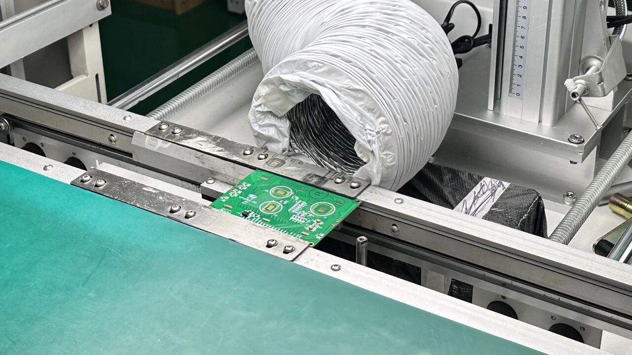
First step on the line: staff perform professional cleaning of the PCB boards that have gone through SMT. Using semi-automated laser cleaning of the gold fingers, dust, oil, impurities, and residual stains are thoroughly removed, ensuring clean pads and an impurity-free board surface.
A clean board is the foundation for high bonding yield, eliminating from the source issues like cold soldering, poor bonding, and contact problems caused by impurities, perfectly paving the way for subsequent IC placement and aluminum wire bonding.
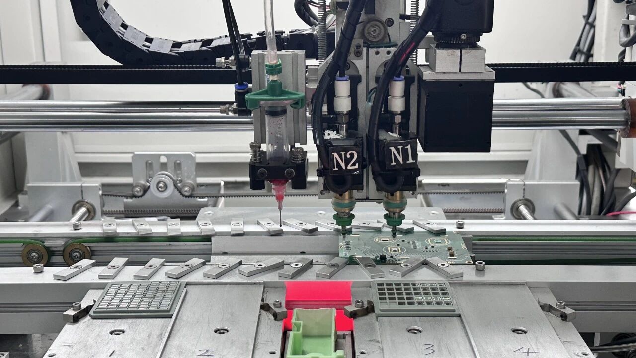
After cleaning, the process moves to the core chip bonding step. The workshop uses high-precision alignment equipment to accurately place the driver IC chip into the designated position on the circuit board. The alignment angle, position, and flatness are strictly controlled to ensure the IC and substrate bond perfectly with precise alignment and zero deviation.
The IC is the "brain" of the LCD module. The precision of this step directly determines the stability of subsequent circuit transmission and is the core foundational process of the entire COB process—allowing no deviation whatsoever.

This is the most cutting-edge core step of the COB process! The fully automatic bonding equipment starts, using ultra-fine aluminum wire, precisely aligned under a microscope, to connect the driver IC pins to the PCB pads one by one.
Micrometer-level precision wire bonding with even wire routing, neat arcs, and full tailored solder joints ensures efficient signal transmission between the IC and circuit board. The equipment operates at high speed with extreme precision, effectively avoiding issues like breaks, using, and broken lines, ensuring each resulting path is a stable transmission "neural channel," so the screen display remains smooth with no flickering or screen issues.

Immediately after wire bonding, a full self-inspection process is carried out, following the quality principle of "each process must self-check." Operators use microscope equipment to examine the state of the wire, firmness, wire routing consistency, and carefully identify issues such as breaks, jumps, shared contacts, unsightly solder joints, or wire displacement.
Problems are identified and corrected on the spot, blocking defective products from within this stage, preventing defects from entering the next stage, effectively increasing overall yields and product stability.

After passing self-inspection, the process enters the professional glue encapsulation protection stage. Fully automatic encapsulation equipment applies precise amounts of glue accurately in the IC, wire, and pad positions with uniform coverage and is ensure no glue leaks and no contact open. The glue encapsulates the core traces and the chip cleanly.
The glue not only fixes the wires and IC in place, preventing disconnection caused by vibration or impact, but also provides effective sealing, dust resistance, oxidation protection, and static dishcarge protection, comprehensively protecting the internal delicate circuits and greatly extending the service life of the LCD module.
After encapsulation, The semi-finished products are then sent together into curing through oven drying equipment for grilling the glue into the desired of revolution. The workshop strictly follows standard temperature control and drying time to allow the protective glue to cure quickly and uniformly, shaping a dense, solid protective layer.
Curing by drying fully stabilizes the encapsulation and protection effect, allowing the glue to bind tightly to the board surface, chip, and wires, preventing any uncured glue, detachment, or bubbles, making the internal circuit structure stronger and product performance more stable.
After passing the entire set of process inspections, the COB semi-finished products are marked with process identification, sorted, and uniformly stored in the warehouse. The workshop implements standardized semi-finished warehouse management, with separated storage, clear records, and moisture-proof and dust-proof storage, properly preserving each semi-finished piece.
Standardized warehouse management ensures smooth material flow for onward assembly, while also reflecting the superb quality of semi-finished good, avoid damage, moisture, or dust accumulation.
Seven meticulous processes, each layer polished, every step strictly controlled, use micrometer-level craftsmanship to create the high-definition picture and stable performance of every LCD module! Zhaoqing Jinpeng Industrial Co., Ltd. specializes in the research, design, production, and sales based on LCD display, enterprise various SMT capable as COB, TAB, COG liquid crystal modules, hundreds on, supplying, personal product and software customization service, welcome.